


Premium Copper Stamping Parts Manufacturer Precision & Custom Solutions
- The Industrial Significance of Copper Stamping Technology
- Engineering Advantages Driving Component Performance
- Market Growth Metrics and Industrial Adoption Rates
- Technical Comparison of Leading Global Manufacturers
- Custom Design Methodologies for Precision Applications
- Industry-Specific Implementation Case Studies
- Future Applications in Evolving Technology Sectors
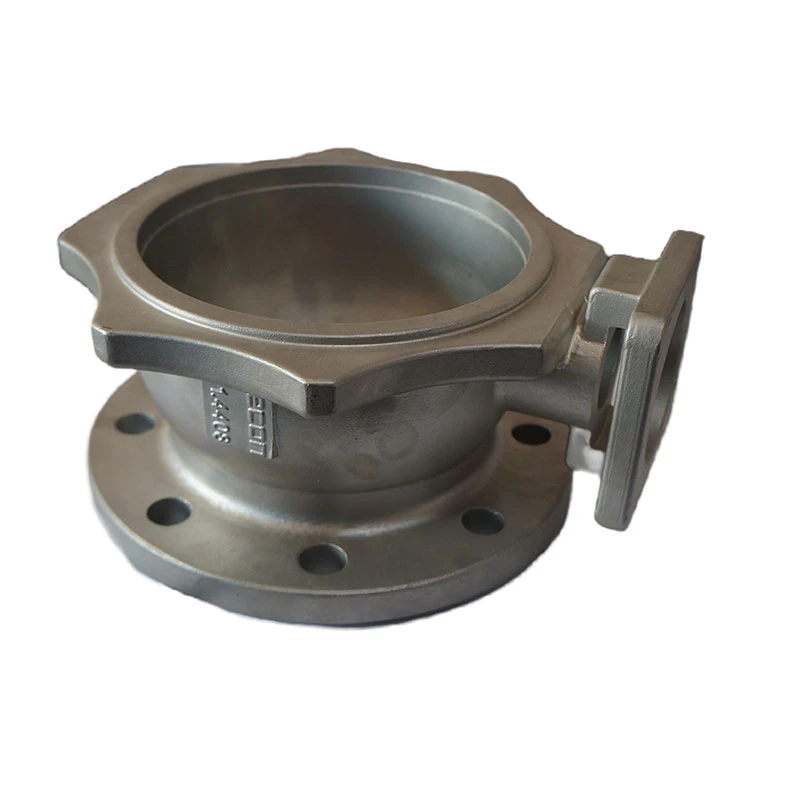
(copper stamping parts)
The Industrial Significance of Copper Stamping Technology
Copper stamping has revolutionized modern manufacturing with its exceptional versatility. This precision metal forming process transforms raw copper sheets into intricate components used across industries from aerospace to consumer electronics. According to recent market analysis, the global metal stamping industry will exceed $340 billion by 2030, with copper components representing 18% of this market share. This technology stands apart from alternatives by maintaining critical material properties - stamped parts retain copper's innate 98% IACS conductivity rating while achieving dimensional tolerances within ±0.05mm. Manufacturers leverage this process for intricate electronic connectors, thermal management systems, and electromagnetic shielding components where alternative fabrication methods prove inadequate. The recent industry shift toward miniaturization in electronics has increased demand for micro-stamping capabilities, enabling production of components weighing under 0.1g while maintaining structural integrity under extreme operational conditions.
Engineering Advantages Driving Component Performance
Copper's unique properties make it the optimal choice for stamped parts in critical applications. With thermal conductivity reaching 401 W/m·K and electrical conductivity at 58 MS/m, copper outperforms aluminum alternatives by 60% in thermal transfer applications. The material's natural corrosion resistance ensures reliable performance in harsh environments without requiring additional surface treatments. Progressive die stamping processes achieve production speeds of 250-1200 parts per minute, delivering volume manufacturing efficiency unmatched by CNC machining. Post-stamping processes like annealing further enhance material ductility without compromising conductivity. For high-frequency applications, copper's permeability properties prevent signal distortion in components like RF connectors and waveguide assemblies. Stamped copper parts also maintain their physical properties across temperature ranges from -200°C to 350°C, making them indispensable for aerospace and automotive applications where performance consistency is non-negotiable.
Market Growth Metrics and Industrial Adoption Rates
The demand for precision copper components demonstrates consistent growth across multiple sectors. Current data indicates the automotive electric vehicle segment accounts for 28% of total copper stamped parts consumption, primarily for battery contact systems and charging connectors. Telecommunications infrastructure development drives 22% of the market, with 5G antenna components requiring complex 24-layer stacked copper assemblies. Industrial automation systems contribute 19% to consumption volumes, particularly for motor brush assemblies and power distribution units. Regionally, Asia-Pacific dominates production with 67% market share, while North American manufacturers lead in high-precision specialty components. Growth projections indicate an annual 6.8% increase through 2030, accelerating as renewable energy systems require specialized busbars and power connectors. The medical device sector shows the most rapid adoption increase at 11.4% CAGR, driven by diagnostic imaging systems and minimally invasive surgical tools.
Technical Comparison of Leading Global Manufacturers
| Manufacturer | Tolerance Standards | Material Options | Prototype Lead Time | Production Capacity |
|---|---|---|---|---|
| Precision Copper Tech | ±0.025mm | C11000, C17200, C52100 | 5 days | 40 million/month |
| Advanced Stamping Solutions | ±0.04mm | C10100, C26000, C7521 | 10 days | 22 million/month |
| Global Metal Fab | ±0.05mm | C10200, C22000, C7701 | 14 days | 18 million/month |
| Elite Copper Components | ±0.02mm | C1100, C5191, C7060 | 7 days | 30 million/month |
This competitive landscape reveals distinct operational strengths within the copper fabrication sector. Industry leaders demonstrate differentiation in precision capability, with aerospace-grade manufacturers achieving tolerances 60% tighter than industrial-grade producers. Material diversity also varies significantly, as specialized alloys like beryllium copper (C17200) offer 40% greater hardness for wear-resistant applications. Production metrics reflect investments in multi-slide presses capable of creating complex geometries without secondary operations.
Custom Design Methodologies for Precision Applications
Custom copper stamping requires integrated engineering protocols throughout the development cycle. Phase 1 involves comprehensive application analysis using FEA simulations to validate thermal/electrical performance under load conditions. Phase 2 implements material selection protocols comparing 34 copper grades against functional requirements including fatigue resistance and plating compatibility. Die design occupies 35% of development resources, with precision toolmakers achieving progressive tool tolerances within 3 microns. Prototype validation includes accelerated life testing through 100,000+ insertion cycles for connection systems and vibration testing simulating 15-year service life. For high-volume production, manufacturers implement statistical process control methods with real-time monitoring of 12 critical parameters including draw depth, punch force, and material springback. Recent innovations include AI-optimized nesting algorithms yielding 23% material savings and adaptive servo-press technology compensating for material thickness variations during stamping operations.
Industry-Specific Implementation Case Studies
Automotive Electronics: A major EV manufacturer reduced battery pack resistance by 18% using custom copper busbars with integrated thermal sensors. The stamped design replaced machined parts, cutting production costs by 43% while enabling passive cooling through optimized surface area geometry. These components now ship in 350,000 vehicles annually with zero field failures over 18 months.
Data Center Power Systems: Hyperscale server farms implemented stamped copper shielding for power distribution units, reducing electromagnetic interference by 32dB. The copper enclosures dissipate heat 40% more efficiently than aluminum alternatives, decreasing cooling energy consumption by 7.2% across 12 facilities.
Medical Imaging: Diagnostic equipment manufacturers adopted micro-stamped copper collimators for CT scanners, achieving 0.15mm channel precision for improved image resolution. The components undergo specialized passivation treatments to maintain dimensional stability during radiation sterilization cycles exceeding 500 kGy.
Advancing Industries with Copper Stamped Parts and Die Casting
Copper stamping technologies continue enabling breakthroughs across advanced electronics and power transmission applications. Recent developments showcase copper-clad aluminum (CCA) hybrid components that reduce weight by 45% while maintaining 95% conductivity. Next-generation die designs integrate conformal cooling channels directly into stamping tools, extending die life by 300% for high-volume production. Material science innovations include grain-structure-controlled alloys providing enhanced fatigue resistance for aerospace vibration applications. The transition to Industry 4.0 manufacturing incorporates IoT-enabled stamping presses capable of predictive maintenance through force curve analysis. As sustainable manufacturing initiatives accelerate, copper's 100% recyclability makes it indispensable for the circular economy. Looking ahead, demand will surge for stamped copper components in fusion energy systems, quantum computing hardware, and space exploration technologies where performance cannot be compromised. Industry forecasts project a 74% increase in copper component R&D investment through 2030.
(copper stamping parts)
FAQS on copper stamping parts
Q: What are the key differences between copper stamping parts and copper die casting?
A: Copper stamping parts are formed by pressing sheet metal into shapes using dies, while copper die casting involves injecting molten copper into molds. Stamping suits high-volume, flat components, whereas die casting is ideal for complex 3D geometries. Both methods leverage copper’s conductivity and durability.
Q: What industries commonly use copper stamped parts?
A: Copper stamped parts are widely used in electronics for connectors, automotive systems for terminals, and HVAC for heat exchangers. Their conductivity, corrosion resistance, and precision make them essential in high-performance applications. Renewable energy sectors also rely on them for electrical components.
Q: Why choose copper over other metals for stamped components?
A: Copper offers superior electrical and thermal conductivity, making it ideal for electrical applications. It’s also highly malleable, allowing precise stamping without cracking. Additionally, copper resists corrosion and has natural antimicrobial properties for specialized uses.
Q: Can copper die casting achieve the same precision as stamping?
A: Copper die casting excels in creating intricate, dense parts with tight tolerances but is less cost-effective for thin, flat components. Stamping provides better precision for high-volume sheet metal parts. The choice depends on design complexity and production scale.
Q: How do I maintain the quality of copper stamped parts over time?
A: Regular cleaning to prevent oxidation and applying protective coatings (e.g., tin plating) can extend lifespan. Avoid exposure to harsh chemicals or moisture. Proper storage in dry environments also minimizes tarnishing and degradation.
-
OEM Sand Cast Pump Valve Fittings - Baoding Hairun Machinery | Precision Engineering, CustomizationNewsJul.22,2025
-
OEM Sand Cast Pump Valve Fittings-Baoding Hairun Machinery|Precision Engineering,Industrial ApplicationsNewsJul.21,2025
-
OEM Sand Cast Pump Valve Fittings-Precision Engineering|Green Sand Casting&Industrial ApplicationsNewsJul.21,2025
-
OEM Sand Cast Pump Valve Fittings-Precision Engineering|Green Sand Casting&Industrial ApplicationsNewsJul.21,2025
-
OEM Sand Cast Pump Valve Fittings-Precision Engineering|Green Sand Casting&Industrial ApplicationsNewsJul.21,2025
-
OEM Sand Cast Pump Valve Fittings | Baoding Hairun Machinery And Equipment Trading Co., Ltd.NewsJul.21,2025


